
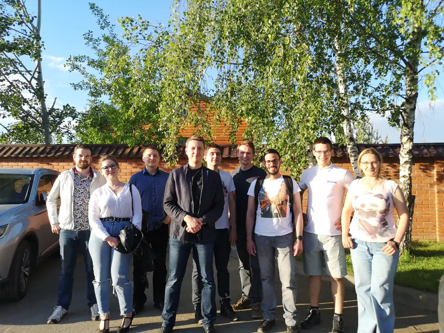
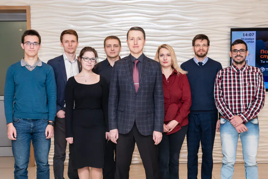
Лаборатория цифрового материаловедения


Наша лаборатория цифрового материаловедения занимается разработкой и применением квантово-химических методов моделирования различных систем на молекулярном уровне. Наши исследования нацелены на решение широкого круга задач, связанных с исследованием механизмов химических реакций, свойств кристаллов, наноматериалов и биомолекул.
Научная группа, состоящая из высококвалифицированных ученых, научных сотрудников и студентов, работает с использованием передовых методов квантово-химического моделирования и разнообразного программного обеспечения, такого как VASP, Siesta, LAMMPS, Gaussian и т.д.
Научно-исследовательская деятельность лаборатории включает в себя проведение экспериментов и анализ результатов с использованием вычислительной химии и методов квантовой механики. Мы занимаемся моделированием химических реакций, количественной оценкой стабильности, прогнозированием свойств материалов, анализом электронных структур, определением параметров кристаллических и молекулярных структур, исследованием связывания лекарственных препаратов с носителями, и тому подобное.
- DFT расчеты
- Молекулярная динамика и квантово-химические расчеты
- Квантовая молекулярная динамика
- Теория квантовой механики/молекулярной механики (КМ/ММ)

Топ-100
Области наук
Журналы


Цитирующие журналы

Цитируемые журналы


Издатели
|
10
20
30
40
50
60
|
|
|
American Chemical Society (ACS)
56 публикаций, 29.17%
|
|
|
Elsevier
31 публикация, 16.15%
|
|
|
Royal Society of Chemistry (RSC)
19 публикаций, 9.9%
|
|
|
MDPI
15 публикаций, 7.81%
|
|
|
Pleiades Publishing
14 публикаций, 7.29%
|
|
|
Springer Nature
11 публикаций, 5.73%
|
|
|
Wiley
11 публикаций, 5.73%
|
|
|
AIP Publishing
11 публикаций, 5.73%
|
|
|
IOP Publishing
6 публикаций, 3.13%
|
|
|
American Physical Society (APS)
5 публикаций, 2.6%
|
|
|
Ivanovo State University of Chemistry and Technology
3 публикации, 1.56%
|
|
|
Uspekhi Fizicheskikh Nauk Journal
2 публикации, 1.04%
|
|
|
Taylor & Francis
1 публикация, 0.52%
|
|
|
American Association for the Advancement of Science (AAAS)
1 публикация, 0.52%
|
|
|
American Scientific Publishers
1 публикация, 0.52%
|
|
|
Siberian Federal University
1 публикация, 0.52%
|
|
|
Beilstein-Institut
1 публикация, 0.52%
|
|
|
The Electrochemical Society
1 публикация, 0.52%
|
|
|
CSIRO Publishing
1 публикация, 0.52%
|
|
|
Autonomous Non-profit Organization Editorial Board of the journal Uspekhi Khimii
1 публикация, 0.52%
|
|
|
10
20
30
40
50
60
|
Организации из публикаций


Страны из публикаций
|
20
40
60
80
100
120
140
160
180
|
|
|
Россия
|
Россия, 180, 93.75%
Россия
180 публикаций, 93.75%
|
|
Япония
|
Япония, 49, 25.52%
Япония
49 публикаций, 25.52%
|
|
США
|
США, 22, 11.46%
США
22 публикации, 11.46%
|
|
Китай
|
Китай, 21, 10.94%
Китай
21 публикация, 10.94%
|
|
Республика Корея
|
Республика Корея, 19, 9.9%
Республика Корея
19 публикаций, 9.9%
|
|
Австралия
|
Австралия, 16, 8.33%
Австралия
16 публикаций, 8.33%
|
|
Финляндия
|
Финляндия, 13, 6.77%
Финляндия
13 публикаций, 6.77%
|
|
Страна не определена
|
Страна не определена, 12, 6.25%
Страна не определена
12 публикаций, 6.25%
|
|
Германия
|
Германия, 12, 6.25%
Германия
12 публикаций, 6.25%
|
|
Венгрия
|
Венгрия, 5, 2.6%
Венгрия
5 публикаций, 2.6%
|
|
Великобритания
|
Великобритания, 4, 2.08%
Великобритания
4 публикации, 2.08%
|
|
Индия
|
Индия, 4, 2.08%
Индия
4 публикации, 2.08%
|
|
Франция
|
Франция, 3, 1.56%
Франция
3 публикации, 1.56%
|
|
Израиль
|
Израиль, 3, 1.56%
Израиль
3 публикации, 1.56%
|
|
Австрия
|
Австрия, 2, 1.04%
Австрия
2 публикации, 1.04%
|
|
Бельгия
|
Бельгия, 2, 1.04%
Бельгия
2 публикации, 1.04%
|
|
Польша
|
Польша, 2, 1.04%
Польша
2 публикации, 1.04%
|
|
Сингапур
|
Сингапур, 2, 1.04%
Сингапур
2 публикации, 1.04%
|
|
Чехия
|
Чехия, 2, 1.04%
Чехия
2 публикации, 1.04%
|
|
Беларусь
|
Беларусь, 1, 0.52%
Беларусь
1 публикация, 0.52%
|
|
Эстония
|
Эстония, 1, 0.52%
Эстония
1 публикация, 0.52%
|
|
Ирландия
|
Ирландия, 1, 0.52%
Ирландия
1 публикация, 0.52%
|
|
Люксембург
|
Люксембург, 1, 0.52%
Люксембург
1 публикация, 0.52%
|
|
Мексика
|
Мексика, 1, 0.52%
Мексика
1 публикация, 0.52%
|
|
Нидерланды
|
Нидерланды, 1, 0.52%
Нидерланды
1 публикация, 0.52%
|
|
ЮАР
|
ЮАР, 1, 0.52%
ЮАР
1 публикация, 0.52%
|
|
20
40
60
80
100
120
140
160
180
|
Цитирующие организации


Цитирующие страны
- Мы не учитываем публикации, у которых нет DOI.
- Статистика пересчитывается раз в сутки.
Направления исследований
Предложен перспективный сорбент для очистки сточных вод от антибиотиков
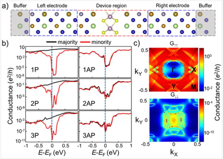
Магнитный туннельный переход на основе полуметаллического сплава Гейслера/МоS2
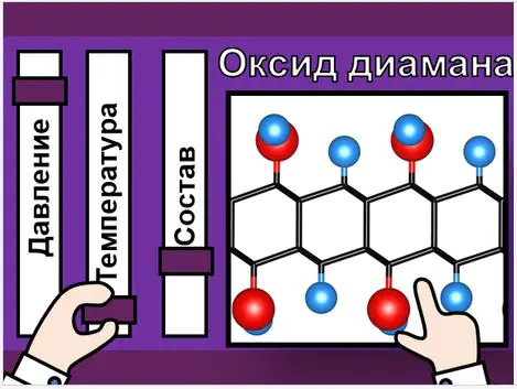
Оксид диамана. Двумерная пленка со смешанным покрытием и разнообразными электронными свойствами
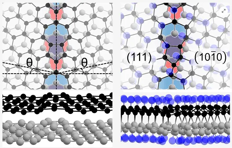
Роль структурных дефектов в росте двумерного алмаза из графена
Края в двухслойном h-BN. Особенности атомной структуры
Полупроводниковые каналы в углеродных нанотрубках с помощью термомеханического изменения хиральности
Экспериментальное и численное исследование наноструктурированных материалов на основе графена и его соединений
Исследование новых классов наноматериалов с необычной структурой: плёнки моноатомной толщины на основе d-металлов и квазиодномерные ван-дер-ваальсовые нанопровода и наноленты состава M2X3 и M2X3Y8
Химически индуцированный фазовый переход в низкоразмерных структурах
Публикации и патенты

Партнёры


")


