Laboratory of superconducting devices for receiving and processing information


Publications
308
Citations
4 068
h-index
32
Authorization required.
Development of superconducting coherent THz band receivers with quantum sensitivity and quantum blue microwave radiation detectors for incoherent receivers. Investigation of THz superconducting generators based on a distributed Josephson junction and their application to receiving systems. Manufacturing of superconducting integrated circuits based on high-quality submicron tunnel junctions with high current density.
- High-frequency measurements
- THz spectroscopy
- Electrophysical measurements
- Radio engineering
Valery Koshelets
Head of Laboratory
Renat Yusupov
Senior Researcher
Artemiy Atepalihin
Junior researcher
Research directions
Development of superconducting coherent THz band receivers with quantum sensitivity
+

The aim of the work in this area is to develop and study THz band superconducting thin-film structures with quantum sensitivity designed for receiving systems of space-based and ground-based radio telescopes. Superconductor-insulator-superconductor (SIS) mixers based on high-quality tunnel junctions are key elements of the most sensitive heterodyne receivers in the MHz band. IC receivers in the ranges 211-275 GHz and 800-950 GHz with a two-band noise temperature (DSB) of about 20 K and 220 K, respectively, have been created and investigated. These developments will be used to create receiving systems for the ground-based telescopes Suffa, APEX and LLMA, as well as for the mission of the Russian Space Agency "Millimetron". Below are photos of the manufactured structures and the results of their research.
Development of quantum SINIS microwave radiation detectors for incoherent receivers
+

Over the past 30 years, a large family of quantum detectors based on the superconductor-insulator- normal metal-superconductor – insulator –superconductor (SINIS) structure has been designed, manufactured and experimentally investigated for operation in the terahertz and sub-THz ranges and bath temperatures up to 50 mK. The key characteristics of detectors based on the SINIS structure and their limiting parameters are closely related to the correct modeling of microwave absorption, power loss, and the balance of electron and phonon cooling. At a frequency of 350 GHz, such detectors demonstrate a current sensitivity of 104 A/W and a noise-equivalent temperature difference (fluctuation sensitivity) of up to 1.6 Μk/√Hz. Detectors with an absorber suspended above the substrate demonstrate a quantum efficiency of 15 electrons per photon.
Modern manufacturing technologies for superconducting detectors, amplifiers, qubits, and quantum computers are in urgent need of research and improvement of the structural and electrophysical parameters of aluminum-based thin films and tunnel junctions. The study of the structure and electrophysical characteristics of films and tunnel junctions is relevant, depending on the methods and modes of manufacturing and obtaining epitaxial films. To achieve these goals, a series of studies will be conducted on the manufacture of film structures using thermal evaporation, magnetron sputtering, and epitaxial growth on heated monocrystalline substrates of different orientations.
As the main result of the work, the authors present the completed development of highly efficient receiving arrays based on SYNIS bolometers of the sub-THZ wavelength range, the characteristics of which, measured in laboratory conditions, meet the requirements of ground-based observatories. The first testing of the developed samples under real background load conditions is expected at the BTA national Observatory (Large Azimuth Telescope) CAO RAN.
A superconducting THz band generator based on a distributed Josephson junction and its application to receiving systems
+

A THz band generator based on a distributed Nb/AlOx/Nb, Nb/AlN/NbN tunnel junction with a characteristic length of 200 to 1000 microns has been developed and successfully applied, providing an output signal of the order of 0.1-2 µW with the possibility of frequency tuning from 200 GHz to 750 GHz. The frequency of the oscillator is controlled by a constant voltage at the junction in accordance with the Josephson ratio f = 2eVDC/h and is limited from above by the fundamental properties of superconducting electrodes, and the signal can be easily stabilized in phase and frequency using a semiconductor phase-lock system.
The phase-stabilized oscillator was successfully used as a source of heterodyne in a superconducting integrated receiver in the 400-700 GHz range with a quantum sensitivity level, on the central microcircuit of which a heterodyne and a receiving mixing system are located simultaneously, while similar receivers in the THz range still use an external source of heterodyne. Many scientific results have been obtained using a superconducting integrated receiver, including: absorption spectra of atmospheric gases, absorption spectra of gases in laboratory conditions, radiation spectra of various sources in the THz range, such as reverse wave lamps, semiconductor microwave signal multipliers, high-temperature BiSrCaCuO superconductors, and others.
In addition, the developed generator was successfully used as a source of a THz signal in an open space by integrating it with a transmitting antenna on a single chip. The presence of radiation harmonics has been experimentally demonstrated. A widely tunable THz generator can be in demand in such fields as weak signal detection, THz microscopy at low temperatures, THz imaging, time and frequency domain spectroscopy, etc.
Manufacturing of superconducting integrated circuits based on high-quality submicron tunnel junctions with high current density
+

Tasks performed:
1. Manufacture of single Nb-AlOx-Nb system structures with a current density of up to 20 kA/cm2.
2. Manufacture of single Nb-AlN-NbN system structures with a current density of up to 200 kA/cm2.
3. Manufacture of NbTiN/SiO2/Al transmission lines with a maximum frequency of 1.2 THz
4. Manufacture of multi-element circuits (up to 1000 pieces) based on Josephson tunnel crossings with barriers made of AlOx and AlN.
5. Manufacture of multilayer (up to 12 layers) planar structures, which include tunnel junctions, screens, transmission lines, anode capacitances, resistors, insulating layers.
The SIS (superconductor-insulator-superconductor) tunnel junction is the main element of most superconducting electronic circuits that can be used to create ultra-sensitive detectors for radio astronomy tasks. Niobium (Nb, Tc=9K) and niobium nitride (NbN, Tc=13-16 K) are used as superconductors for IC transitions. Based on them, Nb-AlOx-Nb type transitions with a maximum frequency of 700 GHz and Nb-AlN-NbN with a maximum frequency of 1.4 THz can be implemented. These three-layer structures are deposited on a quartz or high-resistance silicon substrate using magnetron sputtering systems. Our laboratory has two such magnetron installations: Kurt J. Lesker (6 three-inch DC and RF magnetrons) and Leybol L560 (2 DC magnetrons and 1 RF magnetron with diameters of 5 inches) - Fig. 1 and 2, respectively.
The laboratory has developed a reliable process for manufacturing high-quality micron and submicron-sized SIS junctions (up to 0.5 mm2 using contact photolithography and up to 0.03 mm2 using ELL) with characteristic current densities up to 20kA/cm2 for Nb-AlOx-Nb and up to 200kA/cm2 for Nb-AlN-NbN using the plasmochemical method. and RF etching. Plasma chemical etching using fluorinated gases (CF4, NHF3, SF6) It is carried out in March Jupiter II installations (Fig.3) or Semiteq STE ICP200EF (Fig.4), RF etching in an argon atmosphere can be carried out in Kurt J. Lesker or Semiteq ICP200 installations.
The formation of a given pattern is carried out using a photolithographic process involving Karl Suss MA-150 contact photolithography units (Fig.5) or EM5026-M1 (Fig.6). The technological processes necessary for the manufacture of high-quality tunnel crossings are carried out in clean rooms (purity class ISO6), and critical steps are carried out in laminar cabinets (Figure 7) (purity class ISO5).
Development of technology for manufacturing nanostructures and studying their topology using an electron microscope with the Raith e_LiNE electronic lithography system
+
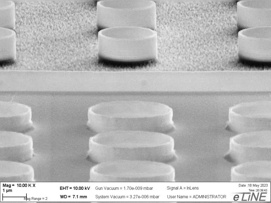
The objectives of the work in this area are both to study the topology and electronic properties of micro- and nano-objects, as well as to create structures in direct lithography mode and in the photomask creation mode.
The e_LiNE electronic lithography system, which is used in the laboratory, combines a scanning electron microscope and an electronic lithography system (a laser interferometric platform and a digital-to-analog converter for controlling the deflection of the electron beam) (Fig. 1). The size of the electron beam is 2 nm for an accelerating voltage of 20 kV. The minimum size of the structure for an ultra-high resolution HSQ resistor is 20 nm.
Publications and patents
Found
Nothing found, try to update filter.

Михаил Александрович Тарасов, Михаил Юрьевич Фоминский, Артем Михайлович Чекушкин, Людмила Викторовна Филиппенко, Валерий Павлович Кошелец
RU2816118,
2024
Михаил Александрович Тарасов, Александра Анатольевна Гунбина, Михаил Юрьевич Фоминский, Артем Михайлович Чекушкин
RU2796347,
2023
Ренат Альбертович Юсупов, Михаил Александрович Тарасов, Валерий Павлович Кошелец, Николай Васильевич Колотинский, Виктор Константинович Корнев
RU2792981,
2023
Михаил Александрович Тарасов, Александра Анатольевна Гунбина, Михаил Юрьевич Фоминский, Артем Михайлович Чекушкин
RU2757762C1,
2021
Михаил Александрович Тарасов, Дарья Владимировна Нагирная, Александра Анатольевна Гунбина, Михаил Юрьевич Фоминский, Ренат Альбертович Юсупов
RU2749575,
2021
Михаил Александрович Тарасов, Дарья Владимировна Нагирная, Александра Анатольевна Гунбина, Михаил Юрьевич Фоминский
RU2733330,
2020
Михаил Александрович Тарасов, Артем Михайлович Чекушкин, Ренат Альбертович Юсупов
RU2685082,
2019
Михаил Александрович Тарасов, Александр Сергеевич Соболев, Артем Михайлович Чекушкин, Ренат Альбертович Юсупов, Александра Анатольевна Гунбина
RU2684897,
2019
Владимир Лейбович Вакс, Елена Георгиевна Домрачева, Николай Вадимович Кинев, Валерий Павлович Кошелец, Сергей Иванович Приползин, Антон Андреевич Яблоков
RU2650354,
2018
Максим Евгеньевич Парамонов, Людмила Викторовна Филиппенко, Михаил Юрьевич Фоминский, Валерий Павлович Кошелец
RU2638964,
2017
Михаил Александрович Тарасов, Артем Михайлович Чекушкин, Ренат Альбертович Юсупов
RU2632630,
2017
2023
—
2026
| Кошелец Валерий Павлович
2023
—
2026
| Юсупов Ренат Альбертович
2023
—
2026
| Худченко Андрей Вячеславович
2023
—
2026
| Тарасов Михаил Александрович
Partners


")
Lab address
г. Москва, ул. Моховая, 11, стр. 7
Authorization required.