
Лаборатория Ультраширокозонных Полупроводников (ЛУШП)


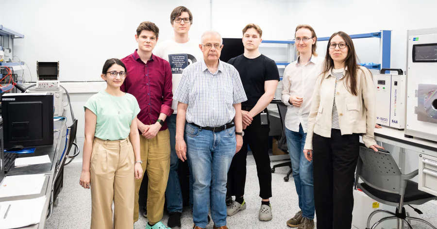
Научно-исследовательской целью проекта является выяснение того, как высокие концентрации точечных дефектов и связанные с ними упругие напряжения в широкозонных полупроводниках на основе оксида галлия могут позволить преодолеть основные недостатки такой системы: низкую теплопроводность, отсутствие примесей или дефектов, создающих эффективную дырочную проводимость, выраженный полиморфизм, сильную метастабильность свойств. Все это на данный момент замедляет внедрение приборов на основе оксида галлия в реальные электронные и оптоэлектронные устройства и мешает коммерциализации технологий на основе данного материала. Ученые научного проекта продемонстрировали возможность изготовления нового материала и эффективного управления его свойствами с помощью экономичной технологии его выращивания. Ga2O3 является перспективной альтернативой кремнию в приборах силовой полупроводниковой электроники и позволяет работать с более высокими напряжениями, при более высоких температурах и с меньшими потерями мощности. Группа профессора Владимира Николаева сумела вырастить толстые пленки α-Ga2O3 с достаточно высоким структурным совершенством и ввести в них примесные атомы олова, поставляющие электроны и изменяющие проводимость пленок в очень широких пределах. Исследователи под руководством профессора Александра Полякова из приготовленных пленок создали тестовые диодные структуры и подробно изучили электронные свойства материала, а также электронную структуру имеющихся в нем примесей и дефектов. Полученные результаты вселяют оптимизм касательно перспектив использования Ga2O3 в силовых приборах, но потребуются очень серьезные дополнительные исследования, чтобы повысить стабильность материала и улучшить его характеристики и их воспроизводимость. Научный коллектив лаборатории ультраширокозонных полупроводников активно сотрудничает с Университетом Корё (Южная Корея), Университетом Осло (Норвегия), университетом Флориды, Институтом Иоффе (Санкт-Петербург), Томским университетом, Курчатовским институтом и др. Лаборатория станет российским координационным центром для исследований фундаментальных свойств и физики устройств на базе широкозонных материалов: оксида галлия, нитридов третьей группы, алмаза, карбида кремния и тд. В частности, в ближайшем будущем усилия будут сосредоточены на комплексных исследованиях системы оксида галлия.
- Адмиттанс-спектроскопия (Admittance Spectroscopy)
- Вольтамперная характеризация
- Релаксационная спектроскопия глубоких уровней (Deep Level Transient Spectroscopy)
- Вольт-фарадное профилирование

Топ-100
Области наук
Журналы


Цитирующие журналы

Цитируемые журналы


Издатели


Организации из публикаций


Страны из публикаций
Цитирующие организации


Цитирующие страны
- Мы не учитываем публикации, у которых нет DOI.
- Статистика пересчитывается раз в сутки.
Направления исследований
Новые радиационные явления в оксиде галлия и их применение в приборах
Публикации и патенты

Партнёры


