
ORËL ResearchLab


Мостович Евгений А
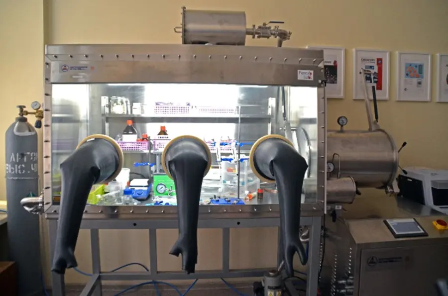
Мы занимаемся разработкой органических полупроводниковых и светоизлучающих материалов для органической электроники - OLED, фотовольтаика и нейроморфные транзисторы. От квантово-химического моделирования и синтеза, до прототипирования устройств.
- Тонкий органический синтез
- Квантово-химическое моделирование оптоэлектронных свойств органических соединений
- УФ-видимая спектроскопия поглощения
- Флуоресцентная Спектроскопия
- Времяразряшенная флуоресценция
- Устройства органической электроники
- Электрохимия
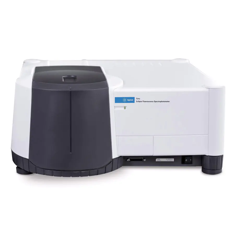
Прибор разрабатывается и выпускается американским производителем Agilent Technologies. Благодаря гибкой функциональности и высокой надежности модель Cary Eclipse применяется для решения различных аналитических задач. С помощью четырех режимов измерения получают высокоточные результаты исследований. Устройство комплектуется волоконно-оптическим зондом, который дает возможность значительно уменьшить время анализа с сохранением корректности данных.
Спектрофлуориметр комплектуется ксеноновой импульсной лампой, благодаря которой осуществляются изучения быстрой кинетики и достигается высокая чувствительность. Пользователь может с высокой точностью регулировать температуру с помощью водяного или Пельтье термостатирования. Благодаря уникальной технологии импульсной ксеноновой лампы в Cary Eclipse исключается фотообесцвечивание пробы. Представленный прибор — единственный флуоресцентный спектрофотометр в своем классе, который имеет иммунитет к засветке наружным освещением.
Топ-100
Области наук
|
2
4
6
8
10
12
|
|
|
General Chemistry
|
General Chemistry, 12, 42.86%
General Chemistry
12 публикаций, 42.86%
|
|
Materials Chemistry
|
Materials Chemistry, 9, 32.14%
Materials Chemistry
9 публикаций, 32.14%
|
|
Organic Chemistry
|
Organic Chemistry, 6, 21.43%
Organic Chemistry
6 публикаций, 21.43%
|
|
Electronic, Optical and Magnetic Materials
|
Electronic, Optical and Magnetic Materials, 5, 17.86%
Electronic, Optical and Magnetic Materials
5 публикаций, 17.86%
|
|
Physical and Theoretical Chemistry
|
Physical and Theoretical Chemistry, 5, 17.86%
Physical and Theoretical Chemistry
5 публикаций, 17.86%
|
|
General Chemical Engineering
|
General Chemical Engineering, 5, 17.86%
General Chemical Engineering
5 публикаций, 17.86%
|
|
Condensed Matter Physics
|
Condensed Matter Physics, 4, 14.29%
Condensed Matter Physics
4 публикации, 14.29%
|
|
Metals and Alloys
|
Metals and Alloys, 3, 10.71%
Metals and Alloys
3 публикации, 10.71%
|
|
Catalysis
|
Catalysis, 3, 10.71%
Catalysis
3 публикации, 10.71%
|
|
Process Chemistry and Technology
|
Process Chemistry and Technology, 3, 10.71%
Process Chemistry and Technology
3 публикации, 10.71%
|
|
General Materials Science
|
General Materials Science, 3, 10.71%
General Materials Science
3 публикации, 10.71%
|
|
Surfaces, Coatings and Films
|
Surfaces, Coatings and Films, 2, 7.14%
Surfaces, Coatings and Films
2 публикации, 7.14%
|
|
General Physics and Astronomy
|
General Physics and Astronomy, 2, 7.14%
General Physics and Astronomy
2 публикации, 7.14%
|
|
Ceramics and Composites
|
Ceramics and Composites, 1, 3.57%
Ceramics and Composites
1 публикация, 3.57%
|
|
Inorganic Chemistry
|
Inorganic Chemistry, 1, 3.57%
Inorganic Chemistry
1 публикация, 3.57%
|
|
Computer Science Applications
|
Computer Science Applications, 1, 3.57%
Computer Science Applications
1 публикация, 3.57%
|
|
Spectroscopy
|
Spectroscopy, 1, 3.57%
Spectroscopy
1 публикация, 3.57%
|
|
Molecular Biology
|
Molecular Biology, 1, 3.57%
Molecular Biology
1 публикация, 3.57%
|
|
General Medicine
|
General Medicine, 1, 3.57%
General Medicine
1 публикация, 3.57%
|
|
Atomic and Molecular Physics, and Optics
|
Atomic and Molecular Physics, and Optics, 1, 3.57%
Atomic and Molecular Physics, and Optics
1 публикация, 3.57%
|
|
Electrical and Electronic Engineering
|
Electrical and Electronic Engineering, 1, 3.57%
Electrical and Electronic Engineering
1 публикация, 3.57%
|
|
Mechanical Engineering
|
Mechanical Engineering, 1, 3.57%
Mechanical Engineering
1 публикация, 3.57%
|
|
General Energy
|
General Energy, 1, 3.57%
General Energy
1 публикация, 3.57%
|
|
Biomaterials
|
Biomaterials, 1, 3.57%
Biomaterials
1 публикация, 3.57%
|
|
Mechanics of Materials
|
Mechanics of Materials, 1, 3.57%
Mechanics of Materials
1 публикация, 3.57%
|
|
2
4
6
8
10
12
|
Журналы
|
1
2
3
|
|
|
Journal of Materials Chemistry C
3 публикации, 10.71%
|
|
|
Dyes and Pigments
3 публикации, 10.71%
|
|
|
RSC Advances
2 публикации, 7.14%
|
|
|
Journal of Organic Chemistry
2 публикации, 7.14%
|
|
|
Journal of Physical Chemistry C
2 публикации, 7.14%
|
|
|
European Journal of Organic Chemistry
2 публикации, 7.14%
|
|
|
New Journal of Chemistry
1 публикация, 3.57%
|
|
|
Physical Chemistry Chemical Physics
1 публикация, 3.57%
|
|
|
Journal of Physics: Conference Series
1 публикация, 3.57%
|
|
|
Mendeleev Communications
1 публикация, 3.57%
|
|
|
Materials Chemistry Frontiers
1 публикация, 3.57%
|
|
|
CrystEngComm
1 публикация, 3.57%
|
|
|
Chemical Communications
1 публикация, 3.57%
|
|
|
Crystal Growth and Design
1 публикация, 3.57%
|
|
|
Acta Crystallographica Section B: Structural Science, Crystal Engineering and Materials
1 публикация, 3.57%
|
|
|
International Journal of Molecular Sciences
1 публикация, 3.57%
|
|
|
Synthetic Metals
1 публикация, 3.57%
|
|
|
ChemPlusChem
1 публикация, 3.57%
|
|
|
Organic Electronics
1 публикация, 3.57%
|
|
|
Arkivoc
1 публикация, 3.57%
|
|
|
1
2
3
|


Цитирующие журналы


Цитируемые журналы


Издатели
|
2
4
6
8
10
|
|
|
Royal Society of Chemistry (RSC)
10 публикаций, 35.71%
|
|
|
Elsevier
5 публикаций, 17.86%
|
|
|
American Chemical Society (ACS)
5 публикаций, 17.86%
|
|
|
Wiley
3 публикации, 10.71%
|
|
|
MDPI
1 публикация, 3.57%
|
|
|
International Union of Crystallography (IUCr)
1 публикация, 3.57%
|
|
|
IOP Publishing
1 публикация, 3.57%
|
|
|
ARKAT USA, Inc.
1 публикация, 3.57%
|
|
|
OOO Zhurnal "Mendeleevskie Soobshcheniya"
1 публикация, 3.57%
|
|
|
2
4
6
8
10
|
Организации из публикаций
|
5
10
15
20
25
|
|
|
Новосибирский Государственный Университет
23 публикации, 82.14%
|
|
|
Новосибирский институт органической химии им. Н.Н. Ворожцова СО РАН
21 публикация, 75%
|
|
|
Институт химической кинетики и горения им. В.В. Воеводского СО РАН
10 публикаций, 35.71%
|
|
|
Институт исследования полимеров Общества Макса Планка
5 публикаций, 17.86%
|
|
|
Франкфуртский университет имени Иоганна Вольфганга Гёте
5 публикаций, 17.86%
|
|
|
Московский государственный университет имени М.В. Ломоносова
3 публикации, 10.71%
|
|
|
Институт Международный томографический центр СО РАН
3 публикации, 10.71%
|
|
|
Институт неорганической химии им. А.В. Николаева СО РАН
3 публикации, 10.71%
|
|
|
Институт физики полупроводников им. А.В. Ржанова СО РАН
3 публикации, 10.71%
|
|
|
Национальный Исследовательский Томский Политехнический Университет
3 публикации, 10.71%
|
|
|
Томский Государственный Университет
2 публикации, 7.14%
|
|
|
Сибирский государственный медицинский университет
2 публикации, 7.14%
|
|
|
Назарбаев Университет
2 публикации, 7.14%
|
|
|
Гронингенский университет
2 публикации, 7.14%
|
|
|
Организация не определена
|
Организация не определена, 1, 3.57%
Организация не определена
1 публикация, 3.57%
|
|
Институт синтетических полимерных материалов им. Н.С. Ениколопова РАН
1 публикация, 3.57%
|
|
|
Высшая школа химической технологии
1 публикация, 3.57%
|
|
|
Ланьчжоуский институт химической физики Китайской академии наук
1 публикация, 3.57%
|
|
|
Грайфсвальдский университет имени Эрнста Морица Арндта
1 публикация, 3.57%
|
|
|
5
10
15
20
25
|


Страны из публикаций
|
5
10
15
20
25
|
|
|
Россия
|
Россия, 25, 89.29%
Россия
25 публикаций, 89.29%
|
|
Германия
|
Германия, 5, 17.86%
Германия
5 публикаций, 17.86%
|
|
Страна не определена
|
Страна не определена, 2, 7.14%
Страна не определена
2 публикации, 7.14%
|
|
Казахстан
|
Казахстан, 2, 7.14%
Казахстан
2 публикации, 7.14%
|
|
Нидерланды
|
Нидерланды, 2, 7.14%
Нидерланды
2 публикации, 7.14%
|
|
Китай
|
Китай, 1, 3.57%
Китай
1 публикация, 3.57%
|
|
Чехия
|
Чехия, 1, 3.57%
Чехия
1 публикация, 3.57%
|
|
5
10
15
20
25
|
Цитирующие организации


Цитирующие страны
- Мы не учитываем публикации, у которых нет DOI.
- Статистика пересчитывается раз в сутки.
