Лаборатория роста тонких пленок и неорганических наноструктур


Лаборатория занимается исследованием процессов роста тонких пленок и неорганических наноструктур. Получением наноструктур полупроводниковых, композитных и металлических соединений, а также исследованием их структуры и свойств.
- Атомно-силовая микроскопия (АСМ)
- Микротвердость
- Рентгенофазовый анализ
- Сканирующая электронная микроскопия (СЭМ)
- Спектроскопия КР (Рамановская)
- Электрохимия
- Молекулярно-слоевое осаждение (Molecular layer deposition)
- Импульсные магнитные поля
- Кинетика фотопроводимости
- Спектроскопия
- Электрофизические измерения
- Энергодисперсионная спектроскопия
- Магнитометрия
- Вакуумно-термическое напыление
- Масс-спектрометрия
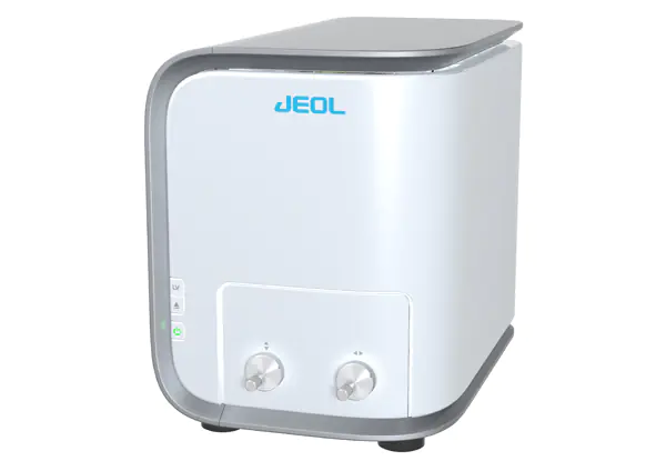
JCM-6000Plus, представляет собой многофункциональный настольный сканирующий микроскоп с сенсорной панелью управления, который отвечает разнообразным потребностям пользователей. JCM-6000Plus оснащен высокочувствительными полупроводниковыми детекторами, используемыми в высококлассных приборах, что упрощает получение информации о контрастности состава образца и обеспечивает эффективный анализ.
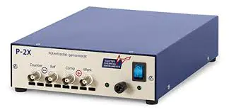
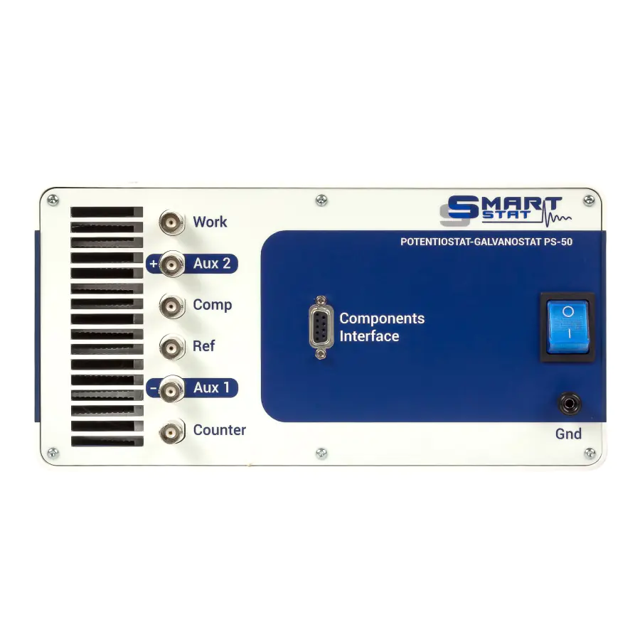
Профессиональный потенциостат-гальваностат PS-50 является бескомпромиссной разработкой, воплотившей в себе все лучшие возможности SmartStat. Одной из ключевых особенностей является наличие шестиэлектродной схемы подключения. Она может быть использована, например, для одновременной регистрации спектров импеданса катода и анода.
Основные особенности:
Потенциостат-гальваностат PS-50 внесен в Госреестр Средств Измерений, номер сертификата 88875-23
Шестиэлектродная схема подключения (2 AUX входа, синхронных с током и потенциалом) в базовой комплектации
Максимально широкий размах рабочих токов и потенциалов
Высококачественный импеданс 50 кГц с возможностью установки FRA до 1.5 МГц
Аналого-цифровой интерфейс SmartStat с двумя аналоговыми входами и цифровым выходом
Наличие IR-компенсации методом ПОС
Потенциостат поставляется с High-End ЦАП разрядностью 20 бит для максимально качественной развертки потенциала (минимальный шаг при синтезе развертки 10 мкВ).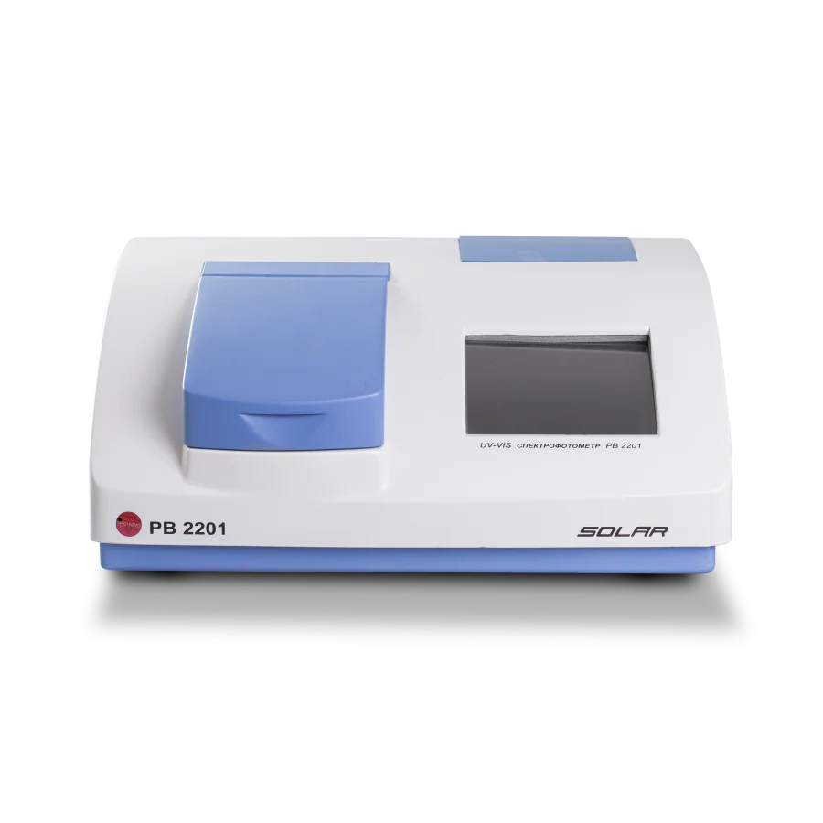
Спектрофотометр UV-VIS PB 2201 ColorCheck – это высокоточный спектрофотометр, который применяется для измерения цветности прозрачных жидкостей или твердых тел. Измерение цветности является важной частью производственного процесса, тк является показателем типа и качества сырья и готовой продукции. Спектр применения прибора крайне широк: нефтехимическая промышленность, пищевая промышленность, химическая и фармацевтическая промышленность, легкая промышленность и др.
Автоматизированная установка для измерения термоэлектрических свойств в нанопленках СТН 300.600.3Omega. Установка предназначена для измерения коэффициента термо-ЭДС, электропроводности и коэффициента теплопроводности в нанопленках. Коэффициент теплопроводности в нанопленках измеряется с помощью 3 омега метода.
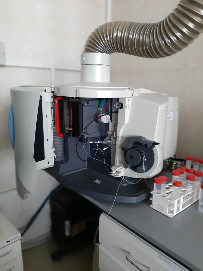
Регистрация эмиссионных спектров различных элементов и дальнейшего расчета содержаний различных элементов на основе полученных спектральных данных.
Прибор для комплексного исследования физико-механических свойств в диапазоне нагрузок до 100 мН. Нанотвердомер оснащен оптическим микроскопом и моторизованным предметным столиком для позиционирования объекта исследования. Высокая степень автоматизации измерений позволяет существенно повысить производительность исследований.
Установка предназначена для проведения следующих экспериментов:
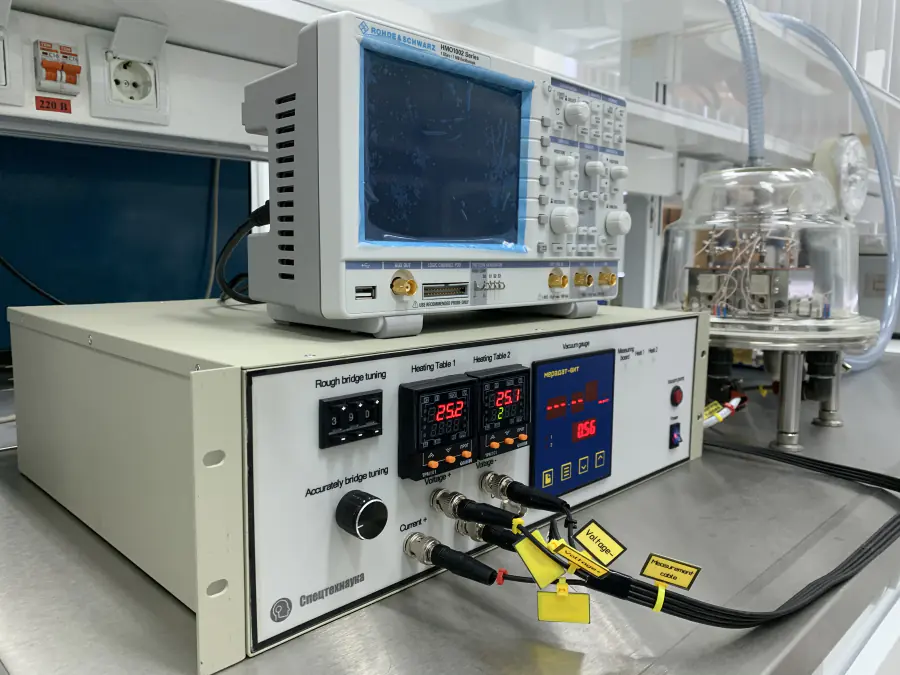
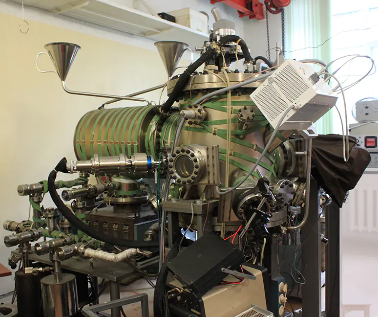
– исследование поверхностных процессов при молекулярно-лучевой эпитаксии на кристалле CdTe методом масс-спектрометрии in situ. Для измерения кинетических параметров используются модулированные молекулярные пучки Cd и Te2.
– изучение начальных стадий роста плёнки CdTe на сапфире и условия зарождения островков при МЛЭ из пучков Cd и Te2.
– исследования начальных стадий роста плёнки Te на сапфире и условия зарождения островков из пучка Te2.
Используемый измерительный комплекс отличается от типичной технологической установки МЛЭ. В камере роста имеются четыре источника молекулярных пучков, два из которых можно модулировать с частотой до 1 кГц. Потоки десорбции с поверхности кристалла регистрируются встроенным масс-спектрометром, что позволяет непосредственно измерять временные характеристики переходных процессов на поверхности кристалла. Знание этих характеристик даёт возможность определять параметры элементарных процессов взаимодействия молекулярных пучков с поверхностью твердых тел (концентрация адсорбированных частиц, время адсорбции, длина диффузионного пробега по поверхности). Именно эти параметры определяют режим роста плёнки, особенно на начальной стадии. Изучение начальных стадий роста плёнок, т. е. процессов происходящих на поверхности подложки при нанесении исходных компонентов получаемых плёнок, позволяет в дальнейшем управлять процессом роста и получать совершенные монокристаллические плёнки.
Процессы конденсации и испарения проходят в неравновесных условиях. Результаты наших экспериментов позволяют предложить модель и рассчитать некоторые кинетические параметры этих неравновесных процессов.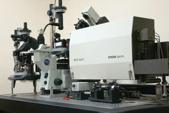
Оборудование позволяет получать информацию о поверхностной структуре материала с пространственным разрешением в нанометровом диапазоне (Исследование топографии, фазового распределения, локальной жесткости, измерение силы адгезии в различных областях материала и т.д.). Также предусматривает возможность изучения физических и химических свойств поверхности образца с большой точностью и высоким разрешением.
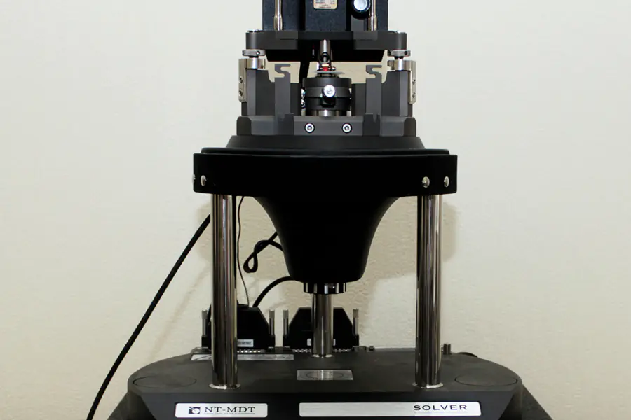
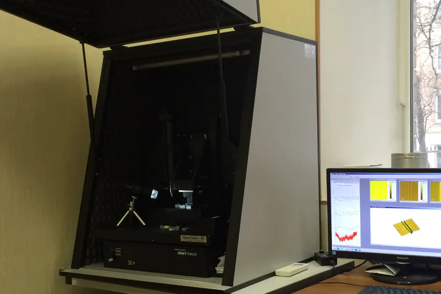
Предназначен для исследования нанобобъектов со сверхвысоким пространственным разрешением (до 0,1 нм по вертикали и до 1 нм по горизонтали). Solver PRO-M позволяет исследовать профиль поверхности образцов с площадью до 100x100 мкм.

Топ-100
Области наук
Журналы


Цитирующие журналы


Цитируемые журналы


Издатели
|
20
40
60
80
100
120
140
|
|
|
Pleiades Publishing
130 публикаций, 73.45%
|
|
|
MDPI
23 публикации, 12.99%
|
|
|
Elsevier
5 публикаций, 2.82%
|
|
|
Wiley
4 публикации, 2.26%
|
|
|
IOP Publishing
4 публикации, 2.26%
|
|
|
Federal Informational-Analytical Center of the Defense Industry
2 публикации, 1.13%
|
|
|
Keldysh Institute of Applied Mathematics
2 публикации, 1.13%
|
|
|
EDP Sciences
1 публикация, 0.56%
|
|
|
AIP Publishing
1 публикация, 0.56%
|
|
|
Image Processing Systems Institute of RAS
1 публикация, 0.56%
|
|
|
Chinese Society of Rare Earths
1 публикация, 0.56%
|
|
|
Institute of Electrical and Electronics Engineers (IEEE)
1 публикация, 0.56%
|
|
|
20
40
60
80
100
120
140
|
Организации из публикаций


Страны из публикаций
|
20
40
60
80
100
120
140
160
180
|
|
|
Россия
|
Россия, 163, 92.09%
Россия
163 публикации, 92.09%
|
|
Страна не определена
|
Страна не определена, 14, 7.91%
Страна не определена
14 публикаций, 7.91%
|
|
Украина
|
Украина, 2, 1.13%
Украина
2 публикации, 1.13%
|
|
США
|
США, 2, 1.13%
США
2 публикации, 1.13%
|
|
Венгрия
|
Венгрия, 2, 1.13%
Венгрия
2 публикации, 1.13%
|
|
СССР
|
СССР, 2, 1.13%
СССР
2 публикации, 1.13%
|
|
Германия
|
Германия, 1, 0.56%
Германия
1 публикация, 0.56%
|
|
Франция
|
Франция, 1, 0.56%
Франция
1 публикация, 0.56%
|
|
Азербайджан
|
Азербайджан, 1, 0.56%
Азербайджан
1 публикация, 0.56%
|
|
Бельгия
|
Бельгия, 1, 0.56%
Бельгия
1 публикация, 0.56%
|
|
Чехия
|
Чехия, 1, 0.56%
Чехия
1 публикация, 0.56%
|
|
20
40
60
80
100
120
140
160
180
|
Цитирующие организации
|
20
40
60
80
100
120
140
160
|
|
|
Курчатовский комплекс "Кристаллография и Фотоника"
147 цитирований, 18.49%
|
|
|
Институт кристаллографии имени А. В. Шубникова
120 цитирований, 15.09%
|
|
|
Организация не определена
|
Организация не определена, 90, 11.32%
Организация не определена
90 цитирований, 11.32%
|
|
Национальный исследовательский центр "Курчатовский институт"
45 цитирований, 5.66%
|
|
|
Дагестанский государственный университет
36 цитирований, 4.53%
|
|
|
Институт физики им. Х.И. Амирханова ДФИЦ РАН
34 цитирования, 4.28%
|
|
|
Дагестанский федеральный исследовательский центр РАН
33 цитирования, 4.15%
|
|
|
Институт кристаллографии
22 цитирования, 2.77%
|
|
|
Московский государственный университет имени М.В. Ломоносова
19 цитирований, 2.39%
|
|
|
Московский педагогический государственный университет
15 цитирований, 1.89%
|
|
|
Национальный исследовательский технологический университет «МИСиС»
13 цитирований, 1.64%
|
|
|
Санкт-Петербургский Политехнический Университет Петра Великого
13 цитирований, 1.64%
|
|
|
Объединенный институт высоких температур РАН
12 цитирований, 1.51%
|
|
|
Физический институт им. П.Н. Лебедева РАН
10 цитирований, 1.26%
|
|
|
Российский Университет Дружбы Народов
10 цитирований, 1.26%
|
|
|
Национальный исследовательский университет «Высшая школа экономики»
9 цитирований, 1.13%
|
|
|
Балтийский Федеральный Университет имени Иммануила Канта
9 цитирований, 1.13%
|
|
|
Уральский федеральный университет имени первого Президента России Б.Н. Ельцина
7 цитирований, 0.88%
|
|
|
Московский физико-технический институт
6 цитирований, 0.75%
|
|
|
Московский государственный технический университет им. Н. Э. Баумана
6 цитирований, 0.75%
|
|
|
Институт общей и неорганической химии им. Н.С. Курнакова РАН
5 цитирований, 0.63%
|
|
|
Институт радиотехники и электроники имени В.А. Котельникова РАН
5 цитирований, 0.63%
|
|
|
Технион - израильский технологический институт
5 цитирований, 0.63%
|
|
|
Национальный университет Ян Мин Цзяотун
5 цитирований, 0.63%
|
|
|
Федеральный исследовательский центр химической физики им. Н.Н. Семёнова РАН
4 цитирования, 0.5%
|
|
|
Сибирский Федеральный Университет
4 цитирования, 0.5%
|
|
|
МИРЭА — Российский технологический университет
4 цитирования, 0.5%
|
|
|
ФИЦ "Красноярский научный центр" СО РАН
4 цитирования, 0.5%
|
|
|
Институт фотонных технологий
4 цитирования, 0.5%
|
|
|
Государственный университет просвещения
4 цитирования, 0.5%
|
|
|
Университет короля Сауда
4 цитирования, 0.5%
|
|
|
Чжэцзянский университет
4 цитирования, 0.5%
|
|
|
Университет Лотарингии
4 цитирования, 0.5%
|
|
|
European Synchrotron Radiation Facility
4 цитирования, 0.5%
|
|
|
Кембриджский университет
4 цитирования, 0.5%
|
|
|
Университет Южной Дании
4 цитирования, 0.5%
|
|
|
Шаньдунский университет
4 цитирования, 0.5%
|
|
|
Немецкий Электронный Синхротрон
4 цитирования, 0.5%
|
|
|
Казанский научный центр РАН
3 цитирования, 0.38%
|
|
|
Институт физики им. Л.В. Киренского СО РАН
3 цитирования, 0.38%
|
|
|
Институт физики металлов имени М. Н. Михеева УрО РАН
3 цитирования, 0.38%
|
|
|
Российский химико-технологический университет имени Д. И. Менделеева
3 цитирования, 0.38%
|
|
|
Казанский физико-технический институт имени Е. К. Завойского КазНЦ РАН
3 цитирования, 0.38%
|
|
|
Институт химии новых материалов НАН Беларуси
3 цитирования, 0.38%
|
|
|
Федеральный исследовательский центр проблем химической физики и медицинской химии РАН
3 цитирования, 0.38%
|
|
|
Сибирский государственный университет науки и технологий им. М.Ф. Решетнева
3 цитирования, 0.38%
|
|
|
Государственный оптический институт имени С. И. Вавилова
3 цитирования, 0.38%
|
|
|
Научно-технологический университет имени короля Абдаллы
3 цитирования, 0.38%
|
|
|
Исламийский колледж в Пешаваре
3 цитирования, 0.38%
|
|
|
Университет Малайя
3 цитирования, 0.38%
|
|
|
Научный Университет Малайзии
3 цитирования, 0.38%
|
|
|
Нанькайский университет
3 цитирования, 0.38%
|
|
|
Северо-Восточный университет
3 цитирования, 0.38%
|
|
|
Педагогический университет Шэньси
3 цитирования, 0.38%
|
|
|
Университетский колледж Лондона
3 цитирования, 0.38%
|
|
|
Бейрутский арабский университет
3 цитирования, 0.38%
|
|
|
Национальный университет Сингапура
3 цитирования, 0.38%
|
|
|
Аргоннская национальная лаборатория
3 цитирования, 0.38%
|
|
|
Ок-Риджская национальная лаборатория
3 цитирования, 0.38%
|
|
|
Автономный университет Мадрида
3 цитирования, 0.38%
|
|
|
Даляньский институт химической физики Китайской академии наук
3 цитирования, 0.38%
|
|
|
Институт физики Чешской академии наук
3 цитирования, 0.38%
|
|
|
Университет Дуйсбурга-Эссена
3 цитирования, 0.38%
|
|
|
Александрийский университет
3 цитирования, 0.38%
|
|
|
Университет Суррея
3 цитирования, 0.38%
|
|
|
Институт ядерной физики Польской академии наук
3 цитирования, 0.38%
|
|
|
Чешский технический университет в Праге
3 цитирования, 0.38%
|
|
|
Институт общей физики имени А.М. Прохорова РАН
2 цитирования, 0.25%
|
|
|
Физико-технический институт им. А.Ф. Иоффе РАН
2 цитирования, 0.25%
|
|
|
Университет ИТМО
2 цитирования, 0.25%
|
|

Санкт-Петербургский Государственный Электротехнический Университет «ЛЭТИ» им. В. И. Ленина
2 цитирования, 0.25%
|
|
|
Южный федеральный университет
2 цитирования, 0.25%
|
|
|
Объединённый институт ядерных исследований
2 цитирования, 0.25%
|
|
|
Санкт-Петербургский государственный университет
2 цитирования, 0.25%
|
|
|
Петербургский институт ядерной физики имени Б. П. Константинова
2 цитирования, 0.25%
|
|
|
Кабардино-Балкарский государственный университет имени Х. М. Бербекова
2 цитирования, 0.25%
|
|
|
Тверской государственный университет
2 цитирования, 0.25%
|
|
|
Карагандинский университет имени академика Е.А. Букетова
2 цитирования, 0.25%
|
|
|
Университет Наджра
2 цитирования, 0.25%
|
|
|
Таифский университет
2 цитирования, 0.25%
|
|
|
Университет принца Мохаммада бин Фахда
2 цитирования, 0.25%
|
|
|
Национальный технологический институт в Хамирпуре
2 цитирования, 0.25%
|
|
|
Саветский институт медицинских и технических наук
2 цитирования, 0.25%
|
|
|
Университет Азад Джамму и Кашмир
2 цитирования, 0.25%
|
|
|
Пекинский педагогический университет
2 цитирования, 0.25%
|
|
|
Институт науки и технологий SRM
2 цитирования, 0.25%
|
|
|
Университет нефти и энергетики
2 цитирования, 0.25%
|
|
|
Университет Йоги Вемана
2 цитирования, 0.25%
|
|
|
Джайнский университет
2 цитирования, 0.25%
|
|
|
Университет Цзилинь
2 цитирования, 0.25%
|
|
|
Университет Шиваджи
2 цитирования, 0.25%
|
|
|
Сианьский университет Цзяотун
2 цитирования, 0.25%
|
|
|
Северо-западный политехнический университет
2 цитирования, 0.25%
|
|
|
Технологический институт Карлсруэ
2 цитирования, 0.25%
|
|
|
Льежский университет
2 цитирования, 0.25%
|
|
|
Центральный южный университет
2 цитирования, 0.25%
|
|
|
Университет Фучжоу
2 цитирования, 0.25%
|
|
|
Национальный университет Сунь Ятсена
2 цитирования, 0.25%
|
|
|
Пекинский научно-технический университет
2 цитирования, 0.25%
|
|
|
Сидяньский университет
2 цитирования, 0.25%
|
|
|
20
40
60
80
100
120
140
160
|
|


Цитирующие страны
- Мы не учитываем публикации, у которых нет DOI.
- Статистика пересчитывается раз в сутки.
Направления исследований
Исследование влияния примесного состава на свойства полупроводниковых твердых растворов на основе CdTe
Получение микро- и наноструктур полупроводников, таких как CdTe, ZnO, SiC, NiО и т.д., а также характеризация полученных микро- и наноструктур
Металл-полимерные композиты на основе полимерных трековых мембран и массивов нанопроволок
Модификация структуры и свойств полупроводниковых соединений с помощью внешних воздействий
Публикации и патенты

Партнёры


