Лаборатория физики и технологии полупроводниковых наногетероструктур для СВЧ-электроники и фотоники (Научная группа технологии гетероструктур)


Лаборатория создана 9 января 2019 г. Основные направления деятельности - Изучение электрофизических свойств разработанных полупроводниковых наногетероструктур. - Изучение структурных, оптических и фотоэлектрических свойств разработанных полупроводниковых твердых растворов. - Разработка изовалентно легированных потенциальных барьеров на основе твердых растворов соединений III- V группы - Термодинамический анализ спинодальных распадов твердых растворов на их устойчивость и упорядочение. - Разработка методов синтеза из жидкой фазы, молекулярных, ионных и атомарных пучков полупроводниковых твердых растворов, а также создания на их основе гетероструктур для оптоэлектронных и фотонных устройств. - Разработка новых полупроводниковых материалов на основе твердых растворов соединений III- V группы. Использование многокомпонентных твердых растворов на основе полупроводниковых соединений AIIIBV в гетероструктурах вызывает все больший интерес исследователей из-за уникальных возможностей этих материалов. Выгодным преимуществом пятикомпонентных твердых растворов перед тройными и четверными является возможность независимого изменения ширины запрещенной зоны и параметра кристаллической решетки. Однако, твердые растворы характеризуются наличием областей спинодальных распадов, что приводит к ограничениям их состава и ширины запрещенной зоны. Увеличение количества компонентов в составе твердых растворов, несомненно, ведет к изменению структурных и оптических свойств таких гетеростурктур и способов их конструирования. Поэтому синтез новых материалов на основе твердых растворов и создание на их основе полупроводниковых гетероинтерфейсов является важной задачей для физики конденсированного состояния и физики полупроводниковых приборов. В этой связи основные направления деятельности лаборатории включают:
- Рентгеновская дифракция
- Атомно-силовая микроскопия (АСМ)
- ИК-спектроскопия
- Спектроскопия КР (Рамановская)
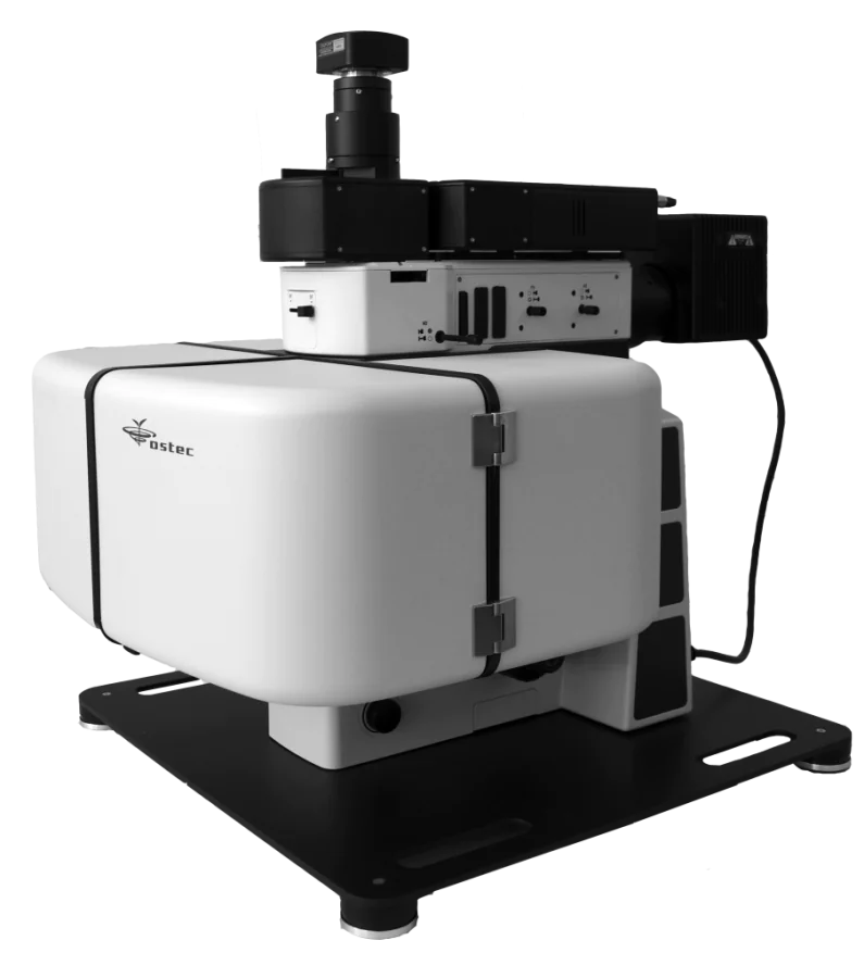
Компактный двухканальный конфокальный рамановский микроскоп RAMOS S120 предназначен для микроспектральных измерений с возможностями на уровне систем высокого класса.
Микроскоп RAMOS S120 имеет жесткую конструкцию без движущихся частей, которая не требует регулировки, обладает как высокой чувствительностью, так и высоким пространственным разрешением.
Широкие возможности, высокая надежность и компактность позволяют использовать RAMOS S120 для решения широкого спектра научных и промышленных задач.
Топ-100
Области наук
|
2
4
6
8
10
12
14
|
|
|
Condensed Matter Physics
|
Condensed Matter Physics, 14, 26.42%
Condensed Matter Physics
14 публикаций, 26.42%
|
|
Electronic, Optical and Magnetic Materials
|
Electronic, Optical and Magnetic Materials, 13, 24.53%
Electronic, Optical and Magnetic Materials
13 публикаций, 24.53%
|
|
Physics and Astronomy (miscellaneous)
|
Physics and Astronomy (miscellaneous), 12, 22.64%
Physics and Astronomy (miscellaneous)
12 публикаций, 22.64%
|
|
Surfaces, Coatings and Films
|
Surfaces, Coatings and Films, 10, 18.87%
Surfaces, Coatings and Films
10 публикаций, 18.87%
|
|
Materials Chemistry
|
Materials Chemistry, 9, 16.98%
Materials Chemistry
9 публикаций, 16.98%
|
|
Metals and Alloys
|
Metals and Alloys, 9, 16.98%
Metals and Alloys
9 публикаций, 16.98%
|
|
Atomic and Molecular Physics, and Optics
|
Atomic and Molecular Physics, and Optics, 8, 15.09%
Atomic and Molecular Physics, and Optics
8 публикаций, 15.09%
|
|
Inorganic Chemistry
|
Inorganic Chemistry, 7, 13.21%
Inorganic Chemistry
7 публикаций, 13.21%
|
|
General Chemical Engineering
|
General Chemical Engineering, 7, 13.21%
General Chemical Engineering
7 публикаций, 13.21%
|
|
General Materials Science
|
General Materials Science, 6, 11.32%
General Materials Science
6 публикаций, 11.32%
|
|
General Physics and Astronomy
|
General Physics and Astronomy, 3, 5.66%
General Physics and Astronomy
3 публикации, 5.66%
|
|
Materials Science (miscellaneous)
|
Materials Science (miscellaneous), 2, 3.77%
Materials Science (miscellaneous)
2 публикации, 3.77%
|
|
Electrical and Electronic Engineering
|
Electrical and Electronic Engineering, 2, 3.77%
Electrical and Electronic Engineering
2 публикации, 3.77%
|
|
Mechanical Engineering
|
Mechanical Engineering, 2, 3.77%
Mechanical Engineering
2 публикации, 3.77%
|
|
Surfaces and Interfaces
|
Surfaces and Interfaces, 2, 3.77%
Surfaces and Interfaces
2 публикации, 3.77%
|
|
General Chemistry
|
General Chemistry, 1, 1.89%
General Chemistry
1 публикация, 1.89%
|
|
Computer Science Applications
|
Computer Science Applications, 1, 1.89%
Computer Science Applications
1 публикация, 1.89%
|
|
General Medicine
|
General Medicine, 1, 1.89%
General Medicine
1 публикация, 1.89%
|
|
Industrial and Manufacturing Engineering
|
Industrial and Manufacturing Engineering, 1, 1.89%
Industrial and Manufacturing Engineering
1 публикация, 1.89%
|
|
General Engineering
|
General Engineering, 1, 1.89%
General Engineering
1 публикация, 1.89%
|
|
Mechanics of Materials
|
Mechanics of Materials, 1, 1.89%
Mechanics of Materials
1 публикация, 1.89%
|
|
Information Systems
|
Information Systems, 1, 1.89%
Information Systems
1 публикация, 1.89%
|
|
Mathematics (miscellaneous)
|
Mathematics (miscellaneous), 1, 1.89%
Mathematics (miscellaneous)
1 публикация, 1.89%
|
|
Business and International Management
|
Business and International Management, 1, 1.89%
Business and International Management
1 публикация, 1.89%
|
|
2
4
6
8
10
12
14
|
Журналы
|
2
4
6
8
10
12
|
|
|
Technical Physics Letters
12 публикаций, 22.64%
|
|
|
Journal of Surface Investigation
8 публикаций, 15.09%
|
|
|
Inorganic Materials
7 публикаций, 13.21%
|
|
|
Semiconductors
7 публикаций, 13.21%
|
|
|
Physics of the Solid State
3 публикации, 5.66%
|
|
|
Thin Solid Films
2 публикации, 3.77%
|
|
|
Beilstein Journal of Nanotechnology
2 публикации, 3.77%
|
|
|
Materials Science Forum
1 публикация, 1.89%
|
|
|
Nanotechnologies in Russia
1 публикация, 1.89%
|
|
|
Journal of Physics: Conference Series
1 публикация, 1.89%
|
|
|
Vacuum
1 публикация, 1.89%
|
|
|
Journal of Nanotechnology
1 публикация, 1.89%
|
|
|
Technical Physics
1 публикация, 1.89%
|
|
|
Crystallography Reports
1 публикация, 1.89%
|
|
|
Kondensirovannye Sredy Mezhfaznye Granitsy (Condensed Matter and Interphases)
1 публикация, 1.89%
|
|
|
Nanosystems: Physics, Chemistry, Mathematics
1 публикация, 1.89%
|
|
|
Scientific and technical journal of information technologies mechanics and optics
1 публикация, 1.89%
|
|
|
Письма в журнал технической физики
1 публикация, 1.89%
|
|
|
2
4
6
8
10
12
|


Цитирующие журналы


Цитируемые журналы


Издатели
|
5
10
15
20
25
30
35
40
|
|
|
Pleiades Publishing
40 публикаций, 75.47%
|
|
|
Elsevier
3 публикации, 5.66%
|
|
|
Beilstein-Institut
2 публикации, 3.77%
|
|
|
ITMO University
2 публикации, 3.77%
|
|
|
Trans Tech Publications
1 публикация, 1.89%
|
|
|
IOP Publishing
1 публикация, 1.89%
|
|
|
Voronezh State University
1 публикация, 1.89%
|
|
|
Hindawi Limited
1 публикация, 1.89%
|
|
|
Ioffe Institute Russian Academy of Sciences
1 публикация, 1.89%
|
|
|
5
10
15
20
25
30
35
40
|
Организации из публикаций
|
5
10
15
20
25
30
35
40
45
50
|
|
|
Южный научный центр РАН
49 публикаций, 92.45%
|
|
|
Южно-Российский государственный политехнический университет (НПИ) имени М. И. Платова
24 публикации, 45.28%
|
|
|
Северо-Кавказский федеральный университет
10 публикаций, 18.87%
|
|
|
Организация не определена
|
Организация не определена, 3, 5.66%
Организация не определена
3 публикации, 5.66%
|
|
Кубанский государственный университет
3 публикации, 5.66%
|
|
|
Физико-технический институт им. А.Ф. Иоффе РАН
1 публикация, 1.89%
|
|
|
Университет Экс-Марсель
1 публикация, 1.89%
|
|
|
Технический университет Ильменау
1 публикация, 1.89%
|
|
|
5
10
15
20
25
30
35
40
45
50
|


Страны из публикаций
|
10
20
30
40
50
|
|
|
Россия
|
Россия, 50, 94.34%
Россия
50 публикаций, 94.34%
|
|
Страна не определена
|
Страна не определена, 5, 9.43%
Страна не определена
5 публикаций, 9.43%
|
|
Германия
|
Германия, 1, 1.89%
Германия
1 публикация, 1.89%
|
|
Франция
|
Франция, 1, 1.89%
Франция
1 публикация, 1.89%
|
|
10
20
30
40
50
|
Цитирующие организации


Цитирующие страны
|
10
20
30
40
50
60
70
80
|
|
|
Россия
|
Россия, 75, 33.33%
Россия
75 цитирований, 33.33%
|
|
Страна не определена
|
Страна не определена, 10, 4.44%
Страна не определена
10 цитирований, 4.44%
|
|
Узбекистан
|
Узбекистан, 7, 3.11%
Узбекистан
7 цитирований, 3.11%
|
|
США
|
США, 3, 1.33%
США
3 цитирования, 1.33%
|
|
Китай
|
Китай, 3, 1.33%
Китай
3 цитирования, 1.33%
|
|
Германия
|
Германия, 2, 0.89%
Германия
2 цитирования, 0.89%
|
|
Франция
|
Франция, 2, 0.89%
Франция
2 цитирования, 0.89%
|
|
Украина
|
Украина, 2, 0.89%
Украина
2 цитирования, 0.89%
|
|
Индия
|
Индия, 2, 0.89%
Индия
2 цитирования, 0.89%
|
|
Литва
|
Литва, 2, 0.89%
Литва
2 цитирования, 0.89%
|
|
Япония
|
Япония, 2, 0.89%
Япония
2 цитирования, 0.89%
|
|
Казахстан
|
Казахстан, 1, 0.44%
Казахстан
1 цитирование, 0.44%
|
|
Португалия
|
Португалия, 1, 0.44%
Португалия
1 цитирование, 0.44%
|
|
Армения
|
Армения, 1, 0.44%
Армения
1 цитирование, 0.44%
|
|
Бангладеш
|
Бангладеш, 1, 0.44%
Бангладеш
1 цитирование, 0.44%
|
|
Испания
|
Испания, 1, 0.44%
Испания
1 цитирование, 0.44%
|
|
Канада
|
Канада, 1, 0.44%
Канада
1 цитирование, 0.44%
|
|
Мексика
|
Мексика, 1, 0.44%
Мексика
1 цитирование, 0.44%
|
|
Республика Корея
|
Республика Корея, 1, 0.44%
Республика Корея
1 цитирование, 0.44%
|
|
Саудовская Аравия
|
Саудовская Аравия, 1, 0.44%
Саудовская Аравия
1 цитирование, 0.44%
|
|
Туркменистан
|
Туркменистан, 1, 0.44%
Туркменистан
1 цитирование, 0.44%
|
|
Турция
|
Турция, 1, 0.44%
Турция
1 цитирование, 0.44%
|
|
10
20
30
40
50
60
70
80
|
- Мы не учитываем публикации, у которых нет DOI.
- Статистика пересчитывается раз в сутки.
Направления исследований
Импульсное лазерное напыление многокомпонентных тонких пленок III-V-Bi
Публикации и патенты

Партнёры

