Лаборатория функциональных материалов и устройств для наноэлектроники


Публикаций
113
Цитирований
2 410
Индекс Хирша
24
Необходимо авторизоваться.
Экспериментальные исследования принципиально новых физических эффектов в наноразмерных структурах на основе неорганических материалов, которые могут быть использованы для разработки синтетических многофункциональных устройств. Такие устройства должны явиться альтернативным подходом к созданию вычислительных систем и информационных технологий принципиально иного уровня.
- Фотолитография
- Электронная и ионная литография
- Осаждение тонких пленок
- Плазмохимическое травление
- Электронная микроскопия
- Электрофизические измерения
- Рентгеновская дифракция
- Рентгеновская спектроскопия с использованием синхротронного излучения
Андрей Зенкевич
Руководитель
Леонид Лев
Старший научный сотрудник
Сергей Зарубин
Научный сотрудник
Никита Сизых
Младший научный сотрудник
Кирилл Трунов
Младший научный сотрудник
Никита Жидков
Младший научный сотрудник
Всего публикаций
46
Всего цитирований
1784
Цитирований на публикацию
38.78
Среднее число публикаций в год
3.83
Годы публикаций
2014-2025 (12 лет)
h-index
20
i10-index
27
m-index
1.67
o-index
72
g-index
42
w-index
7
Описание метрик
h-index
Учёный имеет индекс h, если h из его N статей цитируются как минимум h раз каждая, в то время как оставшиеся (N - h) статей цитируются не более чем h раз каждая.
i10-index
Число статей автора, получивших не менее 10 ссылок каждая.
m-index
m-индекс ученого численно равен отношению его h-индекса к количеству лет, прошедших с момента первой публикации.
o-index
Среднее геометрическое h-индекса и числа цитирований наиболее цитируемой статьи ученого.
g-index
Для данного множества статей, отсортированного в порядке убывания количества цитирований, которые получили эти статьи, g-индекс это наибольшее число, такое что g самых цитируемых статей получили (суммарно) не менее g2 цитирований.
w-index
Если w статей ученого имеют не менее 10w цитирований каждая и другие статьи меньше, чем 10(w+1) цитирований, то w-индекс исследователя равен w.
Топ-100
Области наук
|
2
4
6
8
10
12
14
|
|
|
General Materials Science
|
General Materials Science, 14, 30.43%
General Materials Science
14 публикаций, 30.43%
|
|
Electronic, Optical and Magnetic Materials
|
Electronic, Optical and Magnetic Materials, 13, 28.26%
Electronic, Optical and Magnetic Materials
13 публикаций, 28.26%
|
|
Condensed Matter Physics
|
Condensed Matter Physics, 12, 26.09%
Condensed Matter Physics
12 публикаций, 26.09%
|
|
Electrical and Electronic Engineering
|
Electrical and Electronic Engineering, 8, 17.39%
Electrical and Electronic Engineering
8 публикаций, 17.39%
|
|
Materials Chemistry
|
Materials Chemistry, 6, 13.04%
Materials Chemistry
6 публикаций, 13.04%
|
|
Surfaces, Coatings and Films
|
Surfaces, Coatings and Films, 6, 13.04%
Surfaces, Coatings and Films
6 публикаций, 13.04%
|
|
Physics and Astronomy (miscellaneous)
|
Physics and Astronomy (miscellaneous), 5, 10.87%
Physics and Astronomy (miscellaneous)
5 публикаций, 10.87%
|
|
General Physics and Astronomy
|
General Physics and Astronomy, 4, 8.7%
General Physics and Astronomy
4 публикации, 8.7%
|
|
Mechanical Engineering
|
Mechanical Engineering, 4, 8.7%
Mechanical Engineering
4 публикации, 8.7%
|
|
Surfaces and Interfaces
|
Surfaces and Interfaces, 4, 8.7%
Surfaces and Interfaces
4 публикации, 8.7%
|
|
Mechanics of Materials
|
Mechanics of Materials, 4, 8.7%
Mechanics of Materials
4 публикации, 8.7%
|
|
Metals and Alloys
|
Metals and Alloys, 3, 6.52%
Metals and Alloys
3 публикации, 6.52%
|
|
Atomic and Molecular Physics, and Optics
|
Atomic and Molecular Physics, and Optics, 2, 4.35%
Atomic and Molecular Physics, and Optics
2 публикации, 4.35%
|
|
General Chemistry
|
General Chemistry, 1, 2.17%
General Chemistry
1 публикация, 2.17%
|
|
Ceramics and Composites
|
Ceramics and Composites, 1, 2.17%
Ceramics and Composites
1 публикация, 2.17%
|
|
Computer Science Applications
|
Computer Science Applications, 1, 2.17%
Computer Science Applications
1 публикация, 2.17%
|
|
General Medicine
|
General Medicine, 1, 2.17%
General Medicine
1 публикация, 2.17%
|
|
General Chemical Engineering
|
General Chemical Engineering, 1, 2.17%
General Chemical Engineering
1 публикация, 2.17%
|
|
Polymers and Plastics
|
Polymers and Plastics, 1, 2.17%
Polymers and Plastics
1 публикация, 2.17%
|
|
Bioengineering
|
Bioengineering, 1, 2.17%
Bioengineering
1 публикация, 2.17%
|
|
General Engineering
|
General Engineering, 1, 2.17%
General Engineering
1 публикация, 2.17%
|
|
General Neuroscience
|
General Neuroscience, 1, 2.17%
General Neuroscience
1 публикация, 2.17%
|
|
Artificial Intelligence
|
Artificial Intelligence, 1, 2.17%
Artificial Intelligence
1 публикация, 2.17%
|
|
Cognitive Neuroscience
|
Cognitive Neuroscience, 1, 2.17%
Cognitive Neuroscience
1 публикация, 2.17%
|
|
2
4
6
8
10
12
14
|
Журналы


Цитирующие журналы


Цитируемые журналы


Издатели
|
1
2
3
4
5
6
7
8
9
|
|
|
Elsevier
9 публикаций, 19.57%
|
|
|
Wiley
7 публикаций, 15.22%
|
|
|
American Chemical Society (ACS)
7 публикаций, 15.22%
|
|
|
AIP Publishing
6 публикаций, 13.04%
|
|
|
Pleiades Publishing
3 публикации, 6.52%
|
|
|
IOP Publishing
3 публикации, 6.52%
|
|
|
Royal Society of Chemistry (RSC)
2 публикации, 4.35%
|
|
|
American Physical Society (APS)
2 публикации, 4.35%
|
|
|
Institute of Electrical and Electronics Engineers (IEEE)
2 публикации, 4.35%
|
|
|
Springer Nature
1 публикация, 2.17%
|
|
|
MDPI
1 публикация, 2.17%
|
|
|
Frontiers Media S.A.
1 публикация, 2.17%
|
|
|
American Vacuum Society
1 публикация, 2.17%
|
|
|
1
2
3
4
5
6
7
8
9
|
Организации из публикаций


Страны из публикаций
|
5
10
15
20
25
30
35
40
45
|
|
|
Россия
|
Россия, 44, 95.65%
Россия
44 публикации, 95.65%
|
|
Германия
|
Германия, 13, 28.26%
Германия
13 публикаций, 28.26%
|
|
США
|
США, 6, 13.04%
США
6 публикаций, 13.04%
|
|
Италия
|
Италия, 5, 10.87%
Италия
5 публикаций, 10.87%
|
|
Страна не определена
|
Страна не определена, 3, 6.52%
Страна не определена
3 публикации, 6.52%
|
|
Швейцария
|
Швейцария, 3, 6.52%
Швейцария
3 публикации, 6.52%
|
|
Франция
|
Франция, 1, 2.17%
Франция
1 публикация, 2.17%
|
|
Беларусь
|
Беларусь, 1, 2.17%
Беларусь
1 публикация, 2.17%
|
|
Китай
|
Китай, 1, 2.17%
Китай
1 публикация, 2.17%
|
|
Испания
|
Испания, 1, 2.17%
Испания
1 публикация, 2.17%
|
|
Швеция
|
Швеция, 1, 2.17%
Швеция
1 публикация, 2.17%
|
|
5
10
15
20
25
30
35
40
45
|
Цитирующие организации


Цитирующие страны
- Мы не учитываем публикации, у которых нет DOI.
- Статистика пересчитывается раз в сутки.
Направления исследований
Сегнетоэлектрическая память на основе HfO2
+
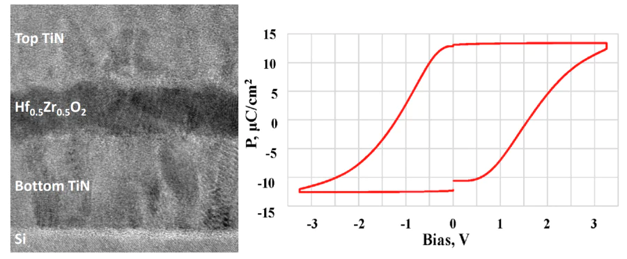
Открытие в 2011 году сегнетоэлектричества (СЭ) в легированных сверхтонких пленках HfO2 возродило интерес исследователей к концепциям микроэлектронных устройств на основе СЭ, поскольку позволило обойти ряд технологических проблем, присущих классическим СЭ материалам, как BaTiO3 и PZT. До настоящего времени интерес лишь усиливался, поскольку успех в научно-исследовательских проектах по СЭ в легированном HfO2 и, особенно, в смешанном Hf0.5Zr0.5O2 позволил вплотную подойти к созданию встроенной СЭ памяти по технологиям FeRAM и FeFET. Наша лаборатория активно участвует как в фундаментальных исследованиях физических механизмов, происходящих в СЭ пленках на основе HfO2, так и в прикладном проекте, направленном на создание полноценных устройств СЭ памяти, производимых в России.
Нейроморфные электронные устройства
+
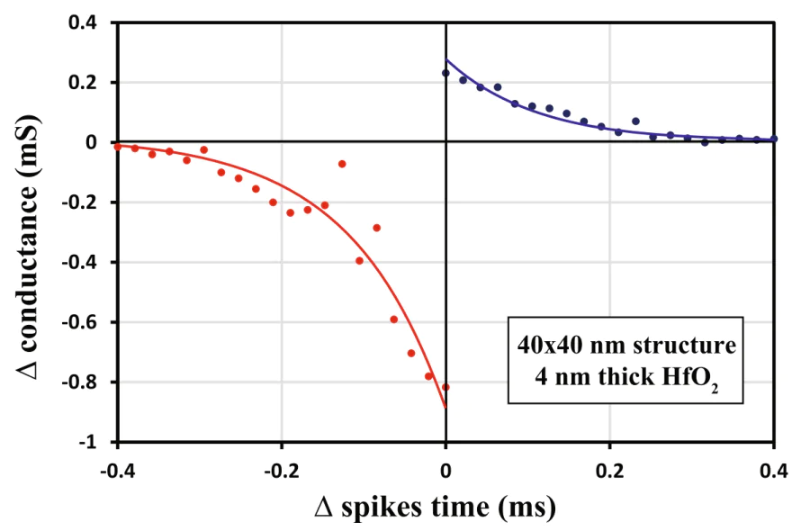
Успех нейронных сетей в последние годы неоспорим и виден уже даже на бытовом уровне. Однако и в этой сфере есть куда расти: создание специализированного "железа", адаптированного под исполнение нейросетевых алгоритмов прямо в чипе, позволит значительно снизить энергопотребление и увеличить скорость работы, а также запускать сложные нейросети на компактных устройствах вместо обращения к удаленным серверам. Наша лаборатория занимается разработкой электронных аналогов синапсов и нейронов, также называемых "мемристорами", как компонентой базы для аппаратной реализации нейронных сетей.
Синхротронные методы исследования материалов и устройств для микроэлектроники
+
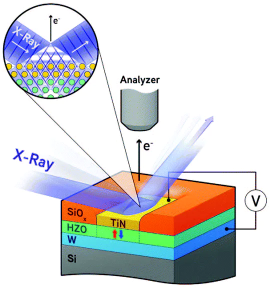
Для исследования новых материалов и создания новых устройств микро- и наноэлектроники требуются все более тонкие и сложные методы. Одним из классов таких методов являются рентгеновская спектроскопия и дифракция с использованием синхротронного излучения. Наша лаборатория обладает уникальными компетенциями в проведении т.н. operando рентгеновских экспериментов, когда измерения происходят непосредственно в процессе работы электронных устройств. Это позволяет наиболее полно характеризовать механизмы функционирования прототипов устройств, оценивать их стабильность во времени и в течение их жизненного цикла. В числе используемых нами методов: рентгеновская фотоэлектронная спектроскопия, спектроскопия рентгеновского поглощения (обе с опцией магнитного дихроизма в излучении с круговой поляризацией), Мёссбауэровская спектроскопия, рентгеновская дифракция.
Новые материалы и устройства
+
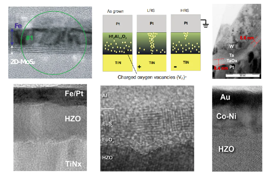
Лаборатория также занимается разработкой методов синтеза новых функциональных материалов в наноразмерных слоях и многослойных структурах, имеющих потенциал приложений в устройствах наноэлектроники, включая: ферромагнитные материалы для спинтроники, оксиды с эффектом обратимого резистивного переключения для устройств памяти и мемристоров, составные мультиферроики для управления магнетизмом при помощи электрических полей. С коллегами из других организаций мы исследуем также двумерные (2D) материалы, топологические изоляторы, галогенидные перовскиты и другие современные твердотельные материалы. Среди методов синтеза новых материалов наша лаборатория особенно специализируется на импульсном лазерном осаждении.
Публикации и патенты
Найдено
Ничего не найдено, попробуйте изменить настройки фильтра.

Юрий Александрович Матвеев, Андрей Владимирович Зенкевич, Дмитрий Владимирович Негров
RU2627125C1,
2017
2024
—
2026
| Ханас Антон Романович
2018
—
2020
| Зенкевич Андрей Владимирович
2014
—
2016
| Зенкевич Андрей Владимирович
2014
—
2016
| Маркеев Андрей Михайлович
Партнёры


Научно исследовательский институт измерительных систем им. Ю.Е. Седакова

Адрес лаборатории
Долгопрудный, Институтский переулок, 9
Необходимо авторизоваться.