Development and research of microelectromechanical systems and semiconductor sensors
Since 2012, the laboratory has been engaged in the development, research and production of microelectromechanical systems (MEMS) and converters based on semiconductor structures. The main physical quantities for measurements are pressure (differential, excess and absolute) and temperature. Pressure sensing elements operating in the range from 0.1 to 16,000 kPa and at temperatures from -60 to +80 ° C with a total measurement error of up to 0.5%, and temperature sensing elements operating with low energy consumption in the range from -60 to +80 ° C with an error of up to 0.8% can be placed together in a small-sized housing.
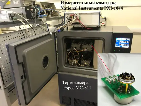
- Measurement of output characteristics of physical quantity converters
Research directions
Circuit design solutions to increase the sensitivity of strain-resistant pressure transducers
+

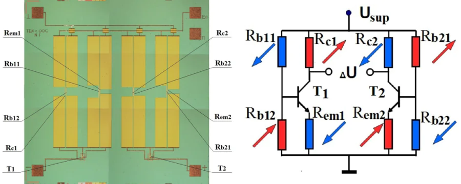
The aim of the work is to develop technical principles for creating strain-resistant pressure transducers based on a circuit design solution to increase sensitivity and minimize overall dimensions while maintaining input conditions for the geometry of the mechanical structure of the membrane, supply voltage and low error rates. Instead of the classical application of an electrical circuit in the form of a Wheatstone strain-resistive bridge, it is proposed to use a circuit in the form of a strain-sensitive differential cascade with negative feedback, where eight p-type conductivity strain gages are located at the places of maximum concentration of mechanical stresses on the membrane of the pressure sensor crystal, which are combined by two bipolar transistors with a vertical structure of n-p-n type of conductivity on a non-deformable crystal regions.
Development and research of a small-sized temperature converter with low energy consumption
+

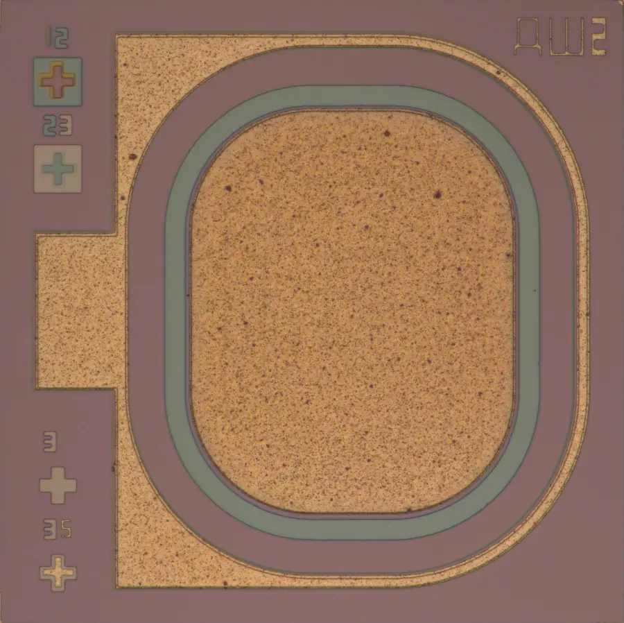
Semiconductor temperature sensors are one of the most demanded elements of the analysis of physical and chemical processes for a wide range of industries and research. Today, temperature sensors are used in nuclear, oil and gas, medical, automotive, aviation, space, metallurgical and many other industries. As a development for joint use with the pressure sensor, the structure of a separate crystal of the temperature sensor in the form of a Schottky diode was chosen, which is formed according to planar technology with the location of the anode and cathode on the same surface (a PDSH crystal with overall dimensions 0,8*0,8*0,4 mm^3). The characteristic of the direct branch of the Schottky diode VAC is determined by the work of the electron output between Mo and n-Si, where, with a supply current Ip = 1 mA, a direct voltage drop of Upr = 208 ± 6 mV is achieved and the temperature coefficient ST = -1.635 ± 0.015 mV/⁰C with linearity kT < 0.4% for the temperature range from -65 to +85 ⁰C. Due to the structure of two p-type guard rings around the perimeter of the anode of the Schottky diode for the reverse branch of the VAC, high breakdown voltage values of Upv > 85 V and low leakage current readings of Iut < 5 µA at 25 ⁰C and Iut < 130 µA at 85 ⁰C (Uobr = 20 V) were obtained.
Development and research of strain gauges of pressure sensors with precision characteristics
+

Pressure sensors (DD) manufactured by FSUE VNIIA are the product of one of the main directions for the serial production of the enterprise for the nuclear and oil and gas industries. The need for continuous improvement of products for specific applications allows us to permanently find and develop new design and technological solutions. The proposed solutions in the vast majority of cases relate to the main element of the DD, which is the DD tensomodule. The DD strain gauge is an assembly structure containing a pressure converter into an electrical signal, made in the form of a microelectromechanical system (MEMS) made of silicon. The pressure converter is manufactured using planar technology with the structure of the electrical circuit of the resistive bridge on the front side and with the formation of a mechanical structure in the form of a complexly profiled membrane on the reverse side. The project solves the main issues related to the causes of the main and additional errors in measuring pressure in the elements, which in fact can be divided into two components - the quality of the implementation of the DD crystal itself and the correctness of the structure of the assembly structure.
Publications and patents
Found
Nothing found, try to update filter.
Михаил Викторович Басов
RU219932U1,
2023
Михаил Викторович Басов
RU219402U1,
2023
Михаил Викторович Басов
RU212796U1,
2022
Михаил Викторович Басов
RU204992U1,
2021
Михаил Викторович Басов
RU202558U1,
2021
Михаил Викторович Басов
RU2730890C1,
2020
Михаил Викторович Басов, Борис Иванович Химушкин
RU195159U1,
2020
Интегральный высокочувствительный элемент преобразователя давления на основе биполярного транзистора
Михаил Викторович Басов, Борис Иванович Химушкин
RU187760U1,
2019
Михаил Викторович Басов, Борис Иванович Химушкин
RU187746U1,
2019
Михаил Викторович Басов, Денис Михайлович Пригодский
RU187531U1,
2019
Михаил Викторович Басов, Борис Иванович Химушкин, Денис Анатольевич Холодков
RU174159U1,
2017
Михаил Викторович Басов
RU167464U1,
2017
Lab address
Москва, Луганская 9
Authorization required.

